


Product Preview DS21Q55
26 of 248 012103
Please contact telecom.support@dalsemi.com or search http://www.maxim-ic.com for updated
information.
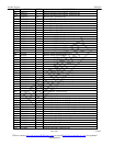
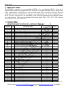
PIN SYMBOL TYPE DESCRIPTION
D2 RSIGF3 O Receive Signaling Freeze Output, Transceiver #3.
V16 RSIGF4 O Receive Signaling Freeze Output, Transceiver #4.
G1 RSYNC1 I/O Receive Sync, Transceiver #1.
D12 RSYNC2 I/O Receive Sync, Transceiver #2.
D1 RSYNC3 I/O Receive Sync, Transceiver #3.
V12 RSYNC4 I/O Receive Sync, Transceiver #4.
H1 RSYSCLK1 I Receive System Clock, Transceiver #1.
F17 RSYSCLK2 I Receive System Clock, Transceiver #2.
G3 RSYSCLK3 I Receive System Clock, Transceiver #3.
W14 RSYSCLK4 I Receive System Clock, Transceiver #4.
Y10 RTIP1 I Receive Analog Tip Input, Transceiver #1.
Y13 RTIP2 I Receive Analog Tip Input, Transceiver #2.
Y16 RTIP3 I Receive Analog Tip Input, Transceiver #3.
Y19 RTIP4 I Receive Analog Tip Input, Transceiver #4.
P1 RVDD1 – Receive Analog Positive Supply.
J17 RVDD2 – Receive Analog Positive Supply.
E4 RVDD3 – Receive Analog Positive Supply.
W18 RVDD4 – Receive Analog Positive Supply.
R2 RVSS1 – Receive Analog Signal Ground
T2 RVSS1 – Receive Analog Signal Ground
H19 RVSS2 – Receive Analog Signal Ground
J18 RVSS2 – Receive Analog Signal Ground
D4 RVSS3 – Receive Analog Signal Ground
D5 RVSS3 – Receive Analog Signal Ground
V20 RVSS4 – Receive Analog Signal Ground
W19 RVSS4 – Receive Analog Signal Ground
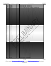
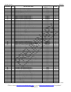
W1 TCHBLK1 O Transmit Channel Block, Transceiver #1.
F20 TCHBLK2 O Transmit Channel Block, Transceiver #2.
C11 TCHBLK3 O Transmit Channel Block, Transceiver #3.
U20 TCHBLK4 O Transmit Channel Block, Transceiver #4.
V10 TCHCLK1 O Transmit Channel Clock, Transceiver #1.
A18 TCHCLK2 O Transmit Channel Clock, Transceiver #2.
B8 TCHCLK3 O Transmit Channel Clock, Transceiver #3.
L18 TCHCLK4 O Transmit Channel Clock, Transceiver #4.
Y9 TCLK1 I Transmit Clock, Transceiver #1.
B19 TCLK2 I Transmit Clock, Transceiver #2.
B10 TCLK3 I Transmit Clock, Transceiver #3.
M19 TCLK4 I Transmit Clock, Transceiver #4.
V6 TCLKI1 I Transmit Clock Input for the LIU, Transceiver #1.
D19 TCLKI2 I Transmit Clock Input for the LIU, Transceiver #2.
C8 TCLKI3 I Transmit Clock Input for the LIU, Transceiver #3.
P20 TCLKI4 I Transmit Clock Input for the LIU, Transceiver #4.
W7 TCLKO1 O Transmit Clock Output from the Framer, Transceiver #1.
E18 TCLKO2 O Transmit Clock Output from the Framer, Transceiver #2.
A7 TCLKO3 O Transmit Clock Output from the Framer, Transceiver #3.
P19 TCLKO4 O Transmit Clock Output from the Fra mer, Transceiver #4.
V3 TLCLK1 O Transmit Link Clock, Transceiver #1.
E20 TLCLK2 O Transmit Link Clock, Transceiver #2.
D6 TLCLK3 O Transmit Link Clock, Transceiver #3.
T18 TLCLK4 O Transmit Link Clock, Transceiver #4.
W5 TLINK1 I Transmit Link Data, Transceiver #1.
E19 TLINK2 I Transmit Link Data, Transceiver #2.