


Product Preview DS21Q55
59 of 248 012103
Please contact telecom.support@dalsemi.com or search http://www.maxim-ic.com for updated
information.
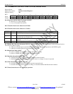
10. COMMON CONTROL AND STATUS REGISTERS
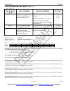
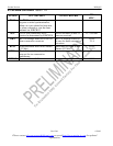
Register Name: CCR1
Register Description: Common Control Register 1
Register Address: 70h
Bit # 7 6 5 4 3 2 1 0
Name - CRC4R SIE ODM DICAI TCSS1 TCSS0 RLOSF
Default 0 0 0 0 0 0 0 0
Bit 0/Function of the RLOS/LOTC Output (RLOSF).
0 = Receive Loss of Sync (RLOS)
1 = Loss of Transmit Clock (LOTC)
Bit 1/Transmit Clock Source Select bit 0 (TCSS0).
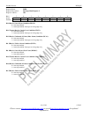
Bit 2/Transmit Clock Source Select bit 1 (TCSS1).
TCSS1 TCSS0 TRANSMIT CLOCK SOURCE
0 0 The TCLK pin is always the source of transmit clock.
0 1 Switch to the clock present at RCLK when the signal at the TCLK pin fails to
transition after one channel time.
1 0 Use the scaled signal present at MCLK as the transmit clock. The TCLK pin is
ignored.
1 1 Use the signal present at RCLK as the transmit clock. The TCLK pin is ignored.
Bit 3/Disable Idle Code Auto Increment (DICAI) Selects/deselects the auto increment feature for the transmit and receive
idle code array address register.
0 = addresses in IAAR register automatically increment on every read/write operation to the PCICR register
1 = addresses in IAAR register do not automatically increment
Bit 4/Output Data Mode (ODM).
0 = pulses at TPOSO and TNEGO are one full TCLKO period wide
1 = pulses at TPOSO and TNEGO are 1/2 TCLKO period wide
Bit 5/Signaling Integration Enable (SIE).
0 = signaling changes of state reported on any change in selected channels
1 = signaling must be stable for three multiframes in order for a change of state to be reported
Bit 6/CRC-4 Recalculate (CRC4R). (E1 Only)
0 = transmit CRC-4 generation and insertion operates in normal mode
1 = transmit CRC-4 generation operates according to G.706 Intermediate Path Recalculation method
Bit 7/Unused, must be set to zero for proper operation.