


Product Preview DS21Q55
158 of 248 012103
Please contact telecom.support@dalsemi.com or search http://www.maxim-ic.com for updated
information.
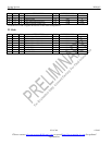
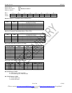
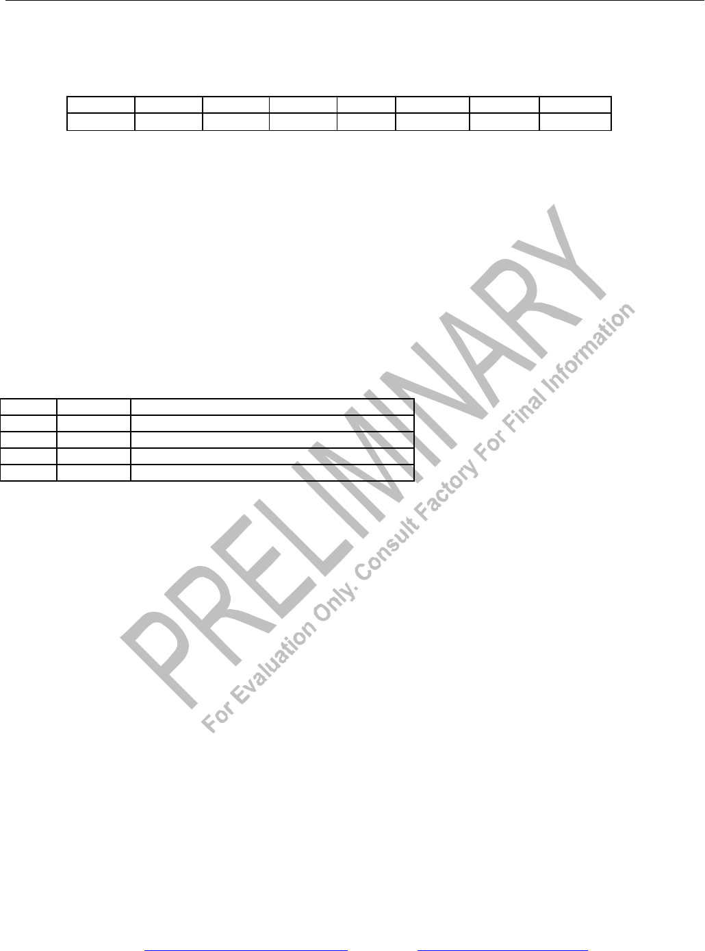
Register Name: LIC3
Register Description: Line Interface Control 3
Register Address: 7Ah
Bit # 7 6 5 4 3 2 1 0
Name - TCES RCES MM1 MM0 RSCLKE TSCLKE TAOZ
Default 0 0 0 0 0 0 0 0
Bit 0/Transmit Alternate Ones and Zeros (TAOZ). Transmit a …101010… pattern (Customer Disconnect Indication
Signal) at TTIP and TRING. The transmission of this data pattern is always timed off of TCLK.
0 = disabled
1 = enabled
Bit 1/Transmit Synchronization G.703 Clock Enable (TSCLKE).
0 = disable 1.544 (T1)/2.048 (E1)MHz transmit synchronization clock
1 = enable 1.544 (T1)/2.048 (E1)MHz transmit synchronization clock
Bit 2/Receive Synchronization G.703 Clock Enable (RSCLKE).
0 = disable 1.544 (T1)/2.048 (E1)MHz synchronization receive mode
1 = enable 1.544 (T1)/2.048 (E1)MHz synchronization receive mode
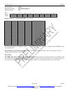
Bits 3 to 4/Monitor Mode (MM0 to MM1).
MM1 MM0 INTERNAL LINEAR GAIN BOOST (dB)
0 0 Normal operation (no boost)
0 1 20
1 0 26
1 1 32
Bit 5/Receive Clock Edge Select (RCES). Selects which RCLKO edge to update RPOSO and RNEGO.
0 = update RPOSO and RNEGO on rising edge of RCLKO
1 = update RPOSO and RNEGO on falling edge of RCLKO
Bit 6/Transmit Clock Edge Select (TCES). Selects which TCLKI edge to sample TPOSI and TNEGI.
0 = sample TPOSI and TNEGI on falling edge of TCLKI
1 = sample TPOSI and TNEGI on rising edge of TCLKI
Bit 7/Unused, must be set to zero for proper operation.