


Product Preview DS21Q55
205 of 248 012103
Please contact telecom.support@dalsemi.com or search http://www.maxim-ic.com for updated
information.
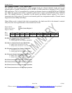
DS21552 0002h
31.2 Test Registers
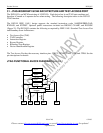
IEEE 1149.1 requires a minimum of two test registers: the bypass register and the boundary scan register.
An optional test register has been included with the DS2155 design. This test register is the identification
register and is used with the IDCODE instruction and the test-logic-reset state of the TAP controller.
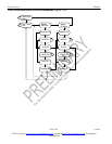
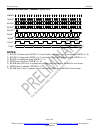
31.3 Boundary Scan Register
This register contains both a shift register path and a latched parallel output for all control cells and
digital I/O cells and is n bits in length. See Table 34-4 for all of the cell bit locations and definitions.
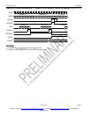
31.4 Bypass Register
This is a single 1-bit shift register used with the BYPASS, CLAMP, and HIGH-Z instructions that
provides a short path between JTDI and JTDO.
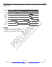
31.5 Identification Register
The identification register contains a 32-bit shift register and a 32-bit latched parallel output. This register
is selected during the IDCODE instruction and when the TAP controller is in the test-logic-reset state.
See Tables 34-2 and 34-3 for more information about bit usage.