


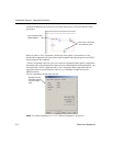
Schematic Capture - Advanced Functions
5-8 Electronics Workbench
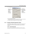
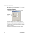
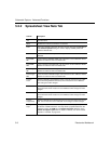
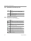
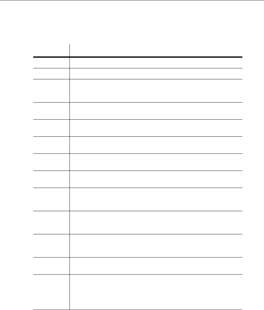
5.2.2 Spreadsheet View Nets Tab
Column Description
Net The net’s name.
Sheet The filename of sheet on which the net is found.
Color Net’s color. “Default” is based on the color scheme selected in the Circuit tab
of the Sheet Properties dialog box. Click to display a Color palette and
select the desired color.
Trace Width Width of the traces after export to PCB layout. Unit of measure is set in
Ultiboard.
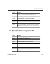
Trace Width
Min
Trace’s minimum allowable width. Unit of measure is set in Ultiboard. Select
desired row and then click in the field to edit.
Trace Width
Max
Trace’s maximum allowable width. Unit of measure is set in Ultiboard. Select
desired row and then click in the field to edit.
Trace Length
Min
Trace’s minimum allowable length. Unit of measure is set in Ultiboard. Select
desired row and then click in the field to edit.
Trace Length
Max
Trace’s maximum allowable length. Unit of measure is set in Ultiboard. Select
desired row and then click in the field to edit.
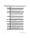
Trace to
Trace
Minimum allowable space between traces in the net and traces in any other
net on the PCB (printed circuit board). Unit of measure is set in Ultiboard.
Click and type to make changes.
Trace to Pad Minimum allowable space between traces in the net and pads on any other
net on the PCB. Unit of measure is set in Ultiboard. Click and type to make
changes.
Trace to Via Minimum allowable space between traces in the net and vias on any other
net on the PCB. Unit of measure is set in Ultiboard. Click and type to make
changes.
Trace to
Copper Area
Minimum allowable space between traces in the net and copper areas on the
PCB. Unit of measure is set in Ultiboard. Click and type to make changes.
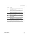
Routing
Layer
The copper layer where the net will be placed. Click to display a drop-down
list with the available selections. This drop-down is populated based on the
selections made in the PCB tab of the Sheet Properties dialog box in the
Number of Copper Layers field. For details on this tab, see “3.4.2.5 Sheet
Properties - PCB Tab” on page 3-30.