


Component Editing
8-20 Electronics Workbench
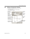
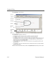
8.5.2.2 Working with the Symbol Editor
To use the Symbol Editor to create working symbols you need to be familiar with the elements
required to make up a symbol in Multicap. The key elements needed for a symbol are:
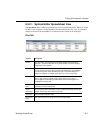
• shape
• pins
These are described in more detail in the following sections.
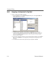
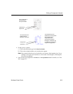
Shape
A symbol requires a shape to allow users to recognize its general function.
You use the drawing capabilities of Multicap’s
Symbol Editor to construct a shape that makes
logical sense for the component you are creating or modifying. The simplest way to do this is
to edit the shape of an existing component. Once this is done, you must add pins.
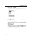
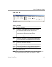
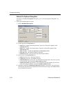
Pins
There are three main parts to a pin. These are the:
•
Name — This is the name of the pin and is usually the same as that given in the data sheet.
For example, most digital parts have pins named “VCC” and “GND”. These names are
used to identify the actual name of the pin in the symbol and must be unique. It is
recommended that you use concise names as they display best on the workspace and on
printed output.
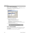
There are two methods to handle components that have more than one pin with the same
name:
1. Have one pin on the symbol that represents the duplicated pin (for example, “GND”)
and match the footprint pins later to the one on the symbol pin.
2. Add multiple pins that have the same basic name but append a digit to represent each
occurence. For example, you could represent multiple ground connections as GND1,
GND2, GND3, etc.
•
Footprint Pin — This is the pin number on the footprint for the device. This numbering
will match the numbering used in PCB layout. Within the
Symbol Editor you only choose
whether to display the footprint pins by default, or not, and their orientation on the
workspace.
•
Shape — The shape of the pin denotes the type of pin. Multicap provides seven pin shapes
that you can use: Line Pin; Dot Pin; Clock Pin; Dot-Clock Pin; Input Wedge Pin; Output
Wedge Pin; Zero-Length Pin. For details, see “ Place Pin Toolbar” on page 8-34. The
shapes are used for identification purposes and do not have any impact on the operation of
the component.
Note The symbol and footprint pins must accurately map in order to transfer correctly to
PCB layout.