


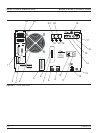
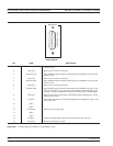
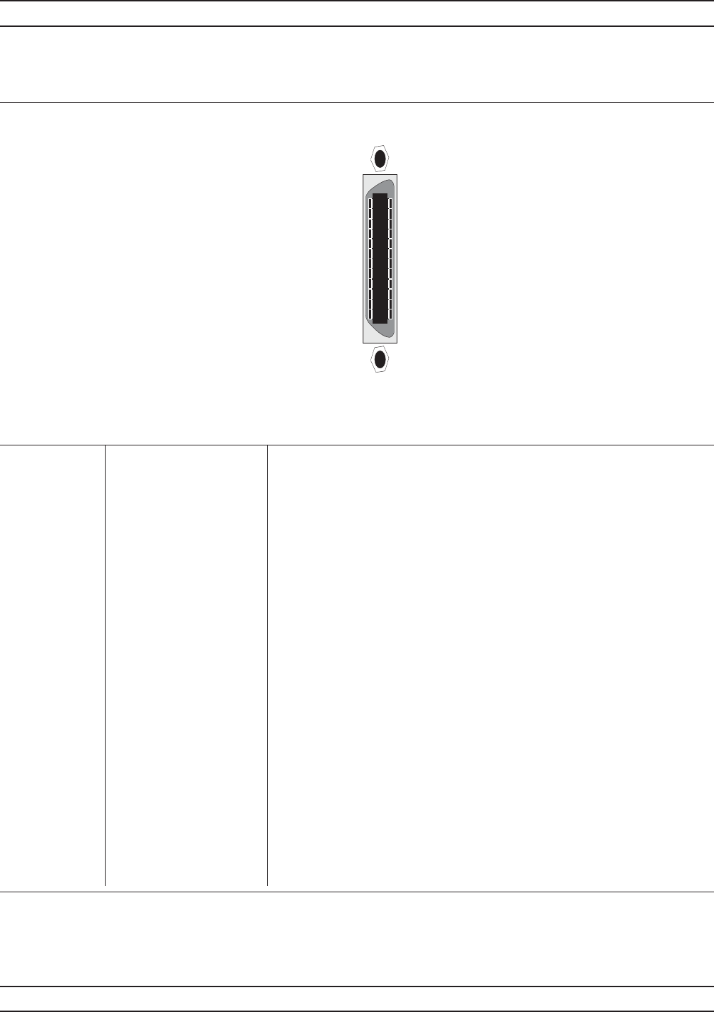
CONNECTOR PINOUT DIAGRAMS REAR PANEL CONNECTORS
B-6 37xxxE OM
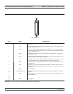
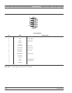
12
11
10
9
8
7
6
5
4
3
2
1
24
23
22
21
20
19
18
17
16
15
14
13
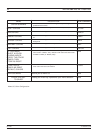
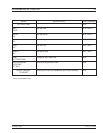
Pinout Diagram
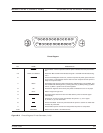
PIN NAME DESCRIPTION
1-4 DIO 1 through DIO 4 Data Input/Output. Bits are HIGH with thedata is logical 0 and LOWwhen the data is
logical 1.
5 EOI End Or Identify. A low-true state indicates that the last byte of a multibyte message
has been placed on the line.
6 DAV Data Valid. A low-true state indicates that the talker has (1) sensed that NRFD is
LOW, (2) placed a byte of data on the bus, and (3) waited an appropriate length of
time for the data to settle.
7 NRFD Not Ready For Data. A high-true state indicates that valid data has not yet been ac
-
cepted by a listener.
8 NDAC Not Data Accepted. A high-false state indicates that the current data byte has been
accepted for internal processing by a listener.
9 IFC Interface Clear. A low-true state places all bus instruments in a known state—such
as, unaddressed to talk, unaddressed to listen, and service request idle.
10 SRQ Service Request. Alow-true state indicates that a bus instrumentneeds service from
the controller.
11 ATN Attention. A low-true state enables the controller to respond to both it’s own lis
-
ten/talk address and to appropriate interface messages— such as, device clear and
serial poll.
12 Shield Chassis ground.
13-16 DIO 5 through DIO 8 Data Input/Output. Bits are high with the data is logical 0 and LOW when the data is
logical 1.
17 REN Remote Enable. A low-true state enables bus instruments to be operated remotely,
when addressed.
18-
24 GND Logic ground.
Figure B-2. Pinout Diagram, GPIB and Dedicated GPIB Connectors