


174 www.xilinx.com Development System Reference Guide
Chapter 9: PAR
R
As the command is performed, PAR records a summary of all placement and routing
iterations in one PAR file at the same level as the directory you specified, then places the
output files (in NCD format) in the specified directory. Also, a Place and Route Report File
and a PAD file are created for each NCD file, describing in detail each individual iteration.
Note:
Reports are formatted for viewing in a monospace (non-proportional) font. If the text editor
you use for viewing the report uses a proportional font, the columns in the report do not line up
correctly. The pad.csv report is formatted for importing into a spreadsheet program or for parsing via
a user script.
Place and Route Report File
The Place and Route report file contains execution information about the PAR command
run. The report file shows the steps taken as the program converges on a placement and
routing solution. A sample PAR report file follows:
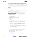
The first lines of the PAR report identify the software version you are running, the machine on
which it is run, and the date and time stamp. In addition, the command line entry is restated,
along with information about the input design files (NCD and PCF). Warning messages also
appear in the first section of the PAR report.
Release 8.1i - par HEAD
Copyright (c) 1995-2005 Xilinx, Inc. All rights reserved.
Par –w –ol high c:\test\test_top_mod_map.ncd c:\test\par0.ncd
c:\test\test_top_mod.pcf
Constraints file: c:\test\test_top_mod.pcf.
Loading device for application Rf_Device from file ‘2vp2.nph’ in envi-
ronment c:/Xilinx.
"test_top_mod" is an NCD, version 1.0, device xc2vp2, package ff672,
speed -7
Initializing temperature to 100.000 Celsius. (default - Range: -40.000
to 100.000 Celsius)
Initializing voltage to 1.500 Volts. (default - Range: 1.400 to 1.600
Volts)
WARNING:Timing:2796 - The input clock clkB_IBUFG to DCM
test_lutram_bram/test_DCM has a period (frequency) specification of
2700 ps (370.37 Mhz). This violates the minimum period (maximum fre-
quency) of 4761 ps (210.04 Mhz).
WARNING:Timing:2798 - The output clock test_lutram_bram/CLK0_W from DCM
test_lutram_bram/test_DCM has a period (frequency) specification of
2700 ps (370.37 Mhz). This violates the minimum period (maximum fre-
quency) of 4761 ps (210.04 Mhz).
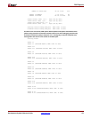
The next section of the PAR report provides a breakdown of the resources in the design and
includes the Device Utilization Summary.
Device speed data version: "PRODUCTION 1.90 2005-12-13".
Device Utilization Summary:
Number of BUFGMUXs 4 out of 16 25%
Number of DCMs 1 out of 4 25%
Number of External IOBs 80 out of 204 39%