


Development System Reference Guide www.xilinx.com 35
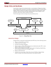
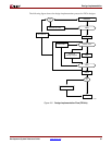
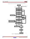
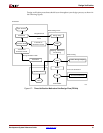
Design Entry and Synthesis
R
HDL Entry and Synthesis
A typical Hardware Description Language (HDL) supports a mixed-level description in
which gate and netlist constructs are used with functional descriptions. This mixed-level
capability enables you to describe system architectures at a high level of abstraction, then
incrementally refine the detailed gate-level implementation of a design.
HDL descriptions offer the following advantages:
• You can verify design functionality early in the design process. A design written as an
HDL description can be simulated immediately. Design simulation at this high level,
at the gate-level before implementation, allows you to evaluate architectural and
design decisions.
• An HDL description is more easily read and understood than a netlist or schematic
description. HDL descriptions provide technology-independent documentation of a
design and its functionality. Because the initial HDL design description is technology
independent, you can use it again to generate the design in a different technology,
without having to translate it from the original technology.
• Large designs are easier to handle with HDL tools than schematic tools.
After you create your HDL design, you must synthesize it. During synthesis, behavioral
information in the HDL file is translated into a structural netlist, and the design is
optimized for a Xilinx device. Xilinx supports HDL synthesis tools for several third-party
synthesis vendors. In addition, Xilinx offers its own synthesis tool, Xilinx Synthesis
Technology (XST). See the Xilinx Synthesis Technology (XST) User Guide for information. For
detailed information on synthesis, see the Synthesis and Simulation Design Guide.
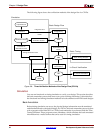
Functional Simulation
After you create your design, you can simulate it. Functional simulation tests the logic in
your design to determine if it works properly. You can save time during subsequent design
steps if you perform functional simulation early in the design flow. See “Simulation” for
more information.
Constraints
You may want to constrain your design within certain timing or placement parameters.
You can specify mapping, block placement, and timing specifications.
You can enter constraints manually or use the Constraints Editor, Floorplanner, or FPGA
Editor, which are graphical user interface (GUI) tools provided by Xilinx. You can use the
Timing Analyzer GUI or TRACE command line program to evaluate the circuit against
these constraints by generating a static timing analysis of your design. See Chapter 12,
“TRACE” and the online Help provided with each GUI for information. See the Constraints
Guide for detailed information on constraints.
Mapping Constraints (FPGAs Only)
You can specify how a block of logic is mapped into CLBs using an FMAP for all Spartan
FPGA and Virtex FPGA families. These mapping symbols can be used in your schematic.
However, if you overuse these specifications, it may be difficult to route your design.