


Development System Reference Guide www.xilinx.com 29
R
Chapter 2
Design Flow
This chapter describes the process for creating, implementing, verifying, and downloading
designs for FPGA and CPLD devices. For a complete description of FPGAs and CPLDs,
refer to the Xilinx Data Sheets at
http://www.xilinx.com/xlnx/xweb/xil_publications_index.jsp
This chapter contains the following sections:
• “Design Flow Overview”
• “Design Entry and Synthesis”
• “Design Implementation”
• “Design Verification”
• “FPGA Design Tips”
Design Flow Overview
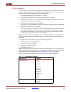
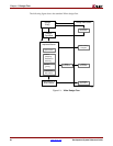
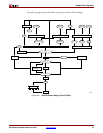
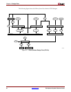
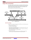
The standard design flow comprises the following steps:
1. Design Entry and Synthesis—In this step of the design flow, you create your design
using a Xilinx-supported schematic editor, a hardware description language (HDL) for
text-based entry, or both. If you use an HDL for text-based entry, you must synthesize
the HDL file into an EDIF file or, if you are using the Xilinx Synthesis Technology
(XST) GUI, you must synthesize the HDL file into an NGC file.
2. Design Implementation—By implementing to a specific Xilinx architecture, you
convert the logical design file format, such as EDIF, that you created in the design
entry and synthesis stage into a physical file format. The physical information is
contained in the native circuit description (NCD) file for FPGAs and the VM6 file for
CPLDs. Then you create a bitstream file from these files and optionally program a
PROM or EPROM for subsequent programming of your Xilinx device.
3. Design Verification—Using a gate-level simulator or cable, you ensure that your
design meets your timing requirements and functions properly. See the iMPACT
online help for information about Xilinx download cables and demonstration boards.
The full design flow is an iterative process of entering, implementing, and verifying your
design until it is correct and complete. The Xilinx Development System allows quick
design iterations through the design flow cycle. Because Xilinx devices permit unlimited
reprogramming, you do not need to discard devices when debugging your design in
circuit.