


Development System Reference Guide www.xilinx.com 223
TRACE Reports
R
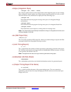
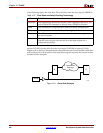
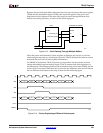
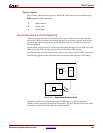
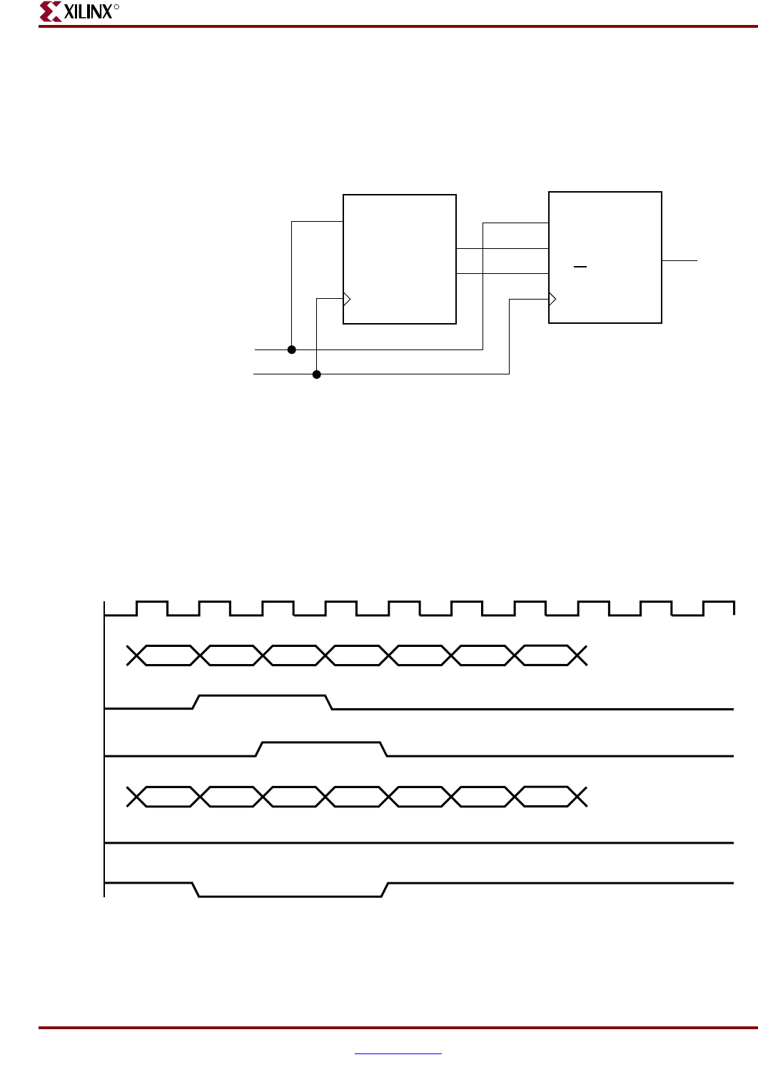
Because the total clock path delay determines the clock arrival times at the source register
(TclkS) and the destination register (TclkD), this check still applies if the source and
destination clocks originate at the same chip input but travel through different clock
buffers and routing resources, as shown in the following figure.
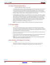
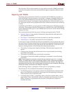
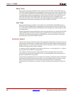
When the source and destination clocks originate at different chip inputs, no obvious
relationship between the two clock inputs exists for TRACE (because the software cannot
determine the clock arrival time or phase information).
For FROM TO constraints, TRACE assumes you have taken into account the external
timing relationship between the chip inputs. TRACE assumes both clock inputs arrive
simultaneously. The difference between the destination clock arrival time (TclkD) and the
source clock arrival time (TclkS) does not account for any difference in the arrival times at
the two different clock inputs to the chip, as shown in the following figure.
Figure 12-3: Clock Passing Through Multiple Buffers
FIFO UP/DOWN COUNTER
RESET
CE
UP/DN
C
BUFCTR_CE
BUFCTR_UPDN
RESET
C
Q
X8261
Figure 12-4: Clocks Originating at Different Device Inputs
C
DIN
X8262
WE
RE
DOUT
FULL
EMPTY
X
DO DI XXXX
X
XDODI X XX