Development System Reference Guide www.xilinx.com 45
Design Verification
R
Timing Simulation
Timing simulation verifies that your design runs at the desired speed for your device
under worst-case conditions. This process is performed after your design is mapped,
placed, and routed for FPGAs or fitted for CPLDs. At this time, all design delays are
known.
Timing simulation is valuable because it can verify timing relationships and determine the
critical paths for the design under worst-case conditions. It can also determine whether or
not the design contains set-up or hold violations.
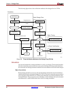
Before you can simulate your design, you must go through the back-annotation process, as
described in “Back-Annotation”. During this process, NetGen creates suitable formats for
various simulators.
Note:
Naming the nets during your design entry is important for both functional and timing
simulation. This allows you to find the nets in the simulations more easily than looking for a software-
generated name.
HDL-Based Simulation
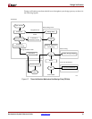
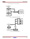
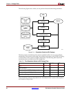
Xilinx supports functional and timing simulation of HDL designs at the following points:
• Register Transfer Level (RTL) simulation, which may include the following:
♦ Instantiated UniSim library components
♦ LogiCORE models
• Post-synthesis functional simulation with one of the following:
♦ Gate-level UniSim library components
♦ Gate-level pre-route SimPrim library components
• Post-implementation back-annotated timing simulation with the following:
♦ SimPrim library components
♦ Standard delay format (SDF) file


