


50 www.xilinx.com Development System Reference Guide
Chapter 2: Design Flow
R
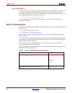
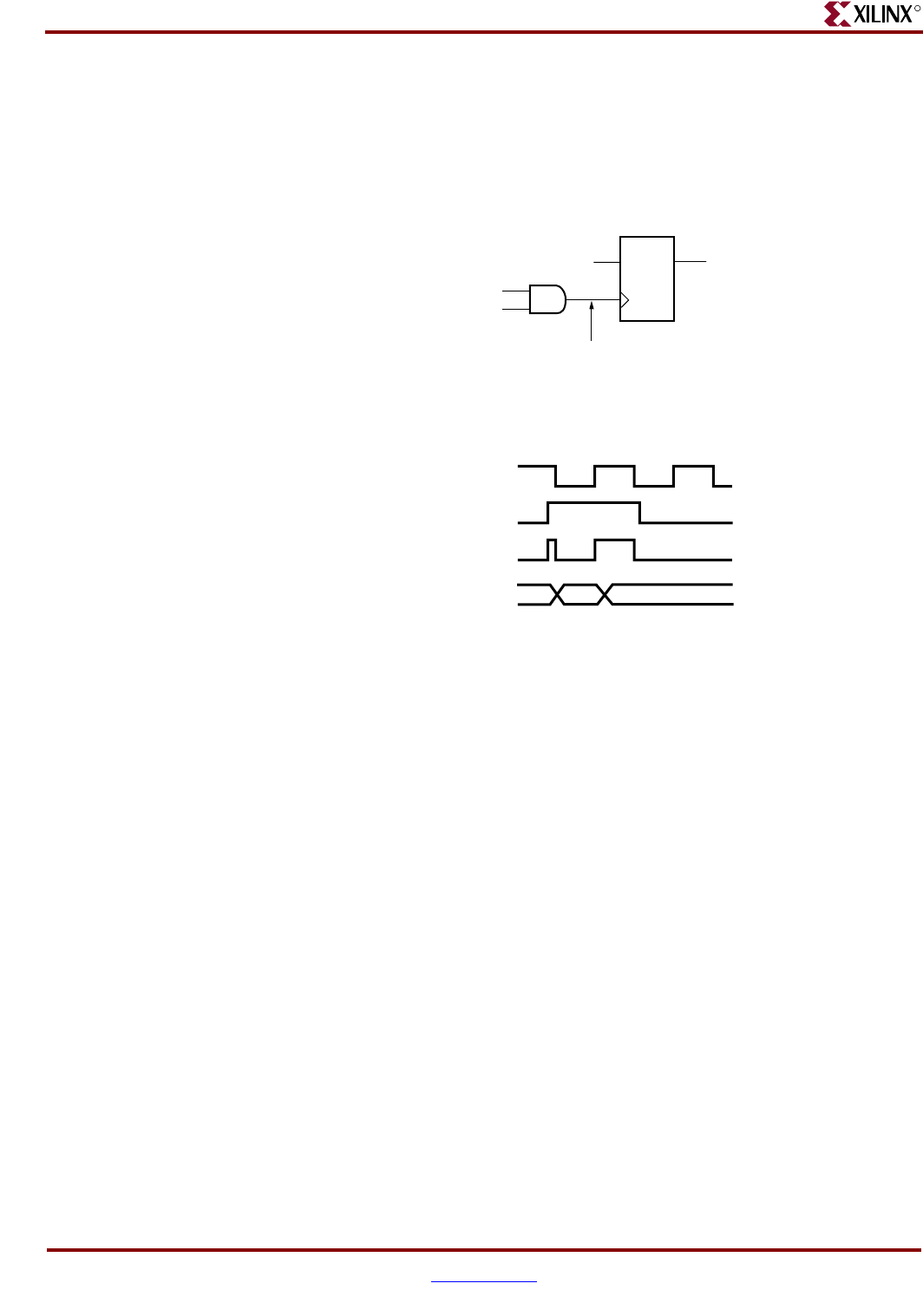
Data Feedback and Clock Enable
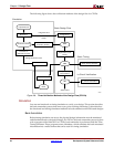
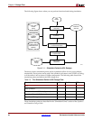
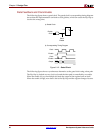
The following figure shows a gated clock. The gated clock’s corresponding timing diagram
shows that this implementation can lead to clock glitches, which can cause the flip-flop to
clock at the wrong time.
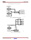
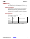
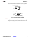
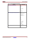
The following figure shows a synchronous alternative to the gated clock using a data path.
The flip-flop is clocked at every clock cycle and the data path is controlled by an enable.
When the enable is Low, the multiplexer feeds the output of the register back on itself.
When the enable is High, new data is fed to the flip-flop and the register changes its state.
Figure 2-12: Gated Clock
X9201
Enable
Clock
DQ
Clock
Enable
Clock
Enable
Output
a) Gated Clock
b) Corresponding Timing Diagram
Clock
Enable