


42 www.xilinx.com Development System Reference Guide
Chapter 2: Design Flow
R
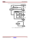
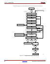
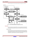
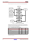
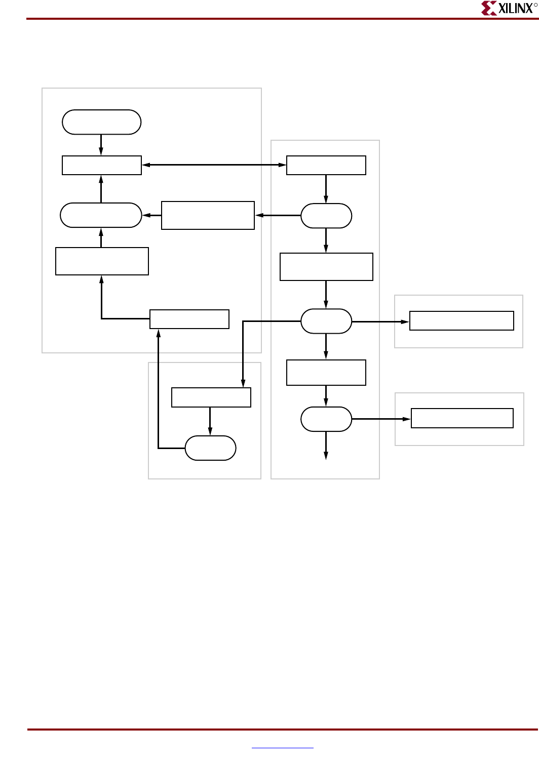
The following figure shows the verification methods of the design flow for CPLDs.
Simulation
You can run functional or timing simulation to verify your design. This section describes
the back-annotation process that must occur prior to timing simulation. It also describes
the functional and timing simulation methods for both schematic and HDL-based designs.
Back-Annotation
Before timing simulation can occur, the physical design information must be translated
and distributed back to the logical design. For FPGAs, this back-annotation process is done
with a program called NetGen. For CPLDs, back-annotation is performed with the TSim
Timing Simulator. These programs create a database, which translates the back-annotated
information into a netlist format that can be used for timing simulation.
Figure 2-8: Three Verification Methods of the Design Flow (CPLDs)
X9538
In-Circuit Verification
Static Timing Analysis
Input Stimulus
Simulation Netlist
Simulation
Xilinx CPLD
Design Entry
Integrated Tool
Functional Simulator
Paths
Timing Simulation Path
Simulation
Static Timing
In-Circuit Verification
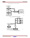
Basic Design Flow
NGD
VM6
Programming
File Creation
JED
Optimization and
Fitting
Translate to
Simulator Format
Translate to
Simulator Format
Back-Annotation
NGA
Translation