


Development System Reference Guide www.xilinx.com 283
BSDLAnno File Composition
R
Explanation:
The only modification that is made to single-ended pins is when the pin is configured
as an input. In this case, the boundary scan logic is disconnected from the output
driver and is unable to drive out on the pin. When a pin is configured as an output, the
boundary scan input register remains connected to that pin. As a result, the boundary
scan logic has the same capabilities as if the pin were configured as a bidirectional pin.
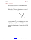
BSDL File Modifications for Differential Pins
If pin 57 is configured as a differential output, differential three-state output, or
differential bidirectional pin, modify as follows:
" 9 (BC_1, *, controlr, 1)," &
" 10 (BC_1, PAD57, output3, X, 9, 1, Z)," &
" 11 (BC_1, PAD57, input, X)," &
If pin 57 is configured as a p-side differential input pin, modify as follows:
" 9 (BC_1, *, internal, 1)," &
" 10 (BC_1, *, internal, X)," &
" 11 (BC_1, PAD57, input, X)," &
If pin 57 is configured as an n-side differential pin (all types: input, output, 3-state
output, and bidirectional), modify as follows:
" 9 (BC_1, *, internal, 1)," &
" 10 (BC_1, *, internal, X)," &
" 11 (BC_1, *, internal, X)," &
Explanation:
All interactions with differential pin pairs are handled by the boundary scan cells
connected to the P-side pin. To capture the value on a differential pair, scan the P-side
input register. To drive a value on a differential pair, shift the value into the P-side
output register. The values in the N-side scan registers have no effect on that pin.
Most boundary scan devices use only three boundary scan registers for each
differential pair. Most devices do not offer direct boundary scan control over each
individual pin, but rather over the two pin pair. This makes sense when you consider
that the two pins are transmitting only one bit of information - hence only one input,
output, and control register is needed. Confusion arises over how differential pins are
handled in Xilinx devices, because there are three boundary scan cells for each pin, or
six registers for the differential pair. The N-side registers remain in the boundary scan
register but are not connected to the pin in any way, which is why the N-side registers
are listed as internal registers in the post-configuration BSDL file. The behavior of the
N-side pin is controlled by the P-side boundary scan registers. For example, when a
value is placed in the P-side output scan register and the output is enabled, the inverse
value is driven onto the N-side pin by the output driver. This is independent from the
Boundary Scan logic.