


Development System Reference Guide www.xilinx.com 49
FPGA Design Tips
R
FPGA Design Tips
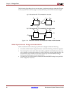
The Xilinx FPGA architecture is best suited for synchronous design. Strict synchronous
design ensures that all registers are driven from the same time base with no clock skew.
This section describes several tips for producing high-performance synchronous designs.
Design Size and Performance
Information about design size and performance can help you to optimize your design.
When you place and route your design, the resulting report files list the number of CLBs,
IOBs, and other device resources available. A first pass estimate can be obtained by
processing the design through the MAP program.
If you want to determine the design size and performance without running automatic
implementation software, you can quickly obtain an estimate from a rough calculation
based on the Xilinx FPGA architecture.
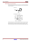
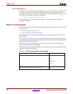
Global Clock Distribution
Xilinx clock networks guarantee small clock skew values. The following table lists the
resources available for the Xilinx FPGA families.
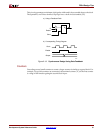
Note:
In certain devices families, global clock buffers are connected to control pin and logic inputs.
If a design requires extensive routing, there may be extra routing delay to these loads.
Table 2-3: Global Clock Resources
FPGA Family Resource Number Destination Pins
Spartan BUFGS 4 Clock, control, or certain input
Virtex, Virtex-E,
Spartan-II,
Spartan-IIE
BUFG 4 Clock
Virtex-II, Virtex-II
Pro
BUFGMUX 16 Clock