


280 www.xilinx.com Development System Reference Guide
Chapter 15: BSDLAnno
R
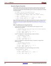
Logical Port Description
The logical port description lists all I/Os on a device and states whether the pin is input,
output, bidirectional, or unavailable for boundary scan. Pins configured as outputs are
described as inout because the input boundary scan cell remains connected, even when the
pin is used only as an output. Describing the output as inout reflects the actual boundary
scan capability of the device and allows for greater test coverage.
Not all I/Os on the die are available (or bonded) in all packages. Unbonded I/Os are
defined in the pre-configuration BSDL file as linkage bits.
For example (from the xcv50e_pq240.bsd file):
port (
CCLK_P179: inout bit;
DONE_P120: inout bit;
GCK0_P92: in bit;
GCK1_P89: in bit;
GCK2_P210: in bit;
GCK3_P213: in bit;
GND: linkage bit_vector (1 to 32);
INIT_P123: inout bit; -- PAD96
IO_P3: inout bit; -- PAD191
IO_P4: inout bit; -- PAD190
IO_P5: inout bit; -- PAD189
IO_P6: inout bit; -- PAD188
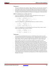
BSDLAnno modifies the logical port description to match the capabilities of the boundary
scan circuitry after configuration. Modifications are made as follows:
• Dedicated pins (JTAG, mode, done, etc.) are not modified; they are left as inout bit.
• Pins defined as bidirectional are left as inout bit
• Pins defined as inputs are changed to in bit
• Pins defined as outputs are left as inout bit
• Unused pins are not modified
• The N-side of differential pairs is changed to linkage bit
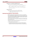
Package Pin-Mapping
Package pin-mapping shows how the pads on the device die are wired to the pins on the
device package.
For example (from the xcv50e_pq240.bsd file):
"CCLK_P179:P179," &
"DONE_P120:P120," &
"GCK0_P92:P92," &
"GCK1_P89:P89," &
"GCK2_P210:P210," &
"GCK3_P213:P213," &
"GND:(P1,P8,P14,P22,P29,P37,P45,P51,P59,P69," &
"P75,P83,P91,P98,P106,P112,P119,P129,P135,P143," &