


Development System Reference Guide www.xilinx.com 47
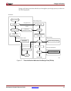
Design Verification
R
The libraries required to support the simulation flows are described in detail in the
“VHDL/Verilog Libraries and Models” section of the Synthesis and Simulation Design
Guide. The flows and libraries support close functional equivalence of initialization
behavior between functional and timing simulations. This is due to the addition of new
methodologies and library cells to simulate Global Set/Reset (GSR) and Global 3-State
(GTS) behavior.
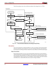
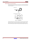
You must address the built-in reset circuitry behavior in your designs, starting with the
first simulation, to ensure that the simulations agree at the three primary points. If you do
not simulate GSR behavior prior to synthesis and place and route, your RTL and
post-synthesis simulations may not initialize to the same state as your post-route timing
simulation. If this occurs, your various design descriptions are not functionally equivalent
and your simulation results do not match.
In addition to the behavioral representation for GSR, you must add a Xilinx
implementation directive. This directive is specifies to the place and route tools to use the
special purpose GSR net that is pre-routed on the chip, and not to use the local
asynchronous set/reset pins. Some synthesis tools can identify the GSR net from the
behavioral description, and place the STARTUP module on the net to direct the
implementation tools to use the global network. However, other synthesis tools interpret
behavioral descriptions literally and introduce additional logic into your design to
implement a function. Without specific instructions to use device global networks, the
Xilinx implementation tools use general-purpose logic and interconnect resources to
redundantly build functions already provided by the silicon.
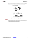
Even if GSR behavior is not described, the chip initializes during configuration, and the
post-route netlist has a net that must be driven during simulation. The “Understanding the
Global Signals for Simulation” section of the Synthesis and Simulation Design Guide includes
the methodology to describe this behavior, as well as the GTS behavior for output buffers.
Xilinx VHDL simulation supports the VITAL standard. This standard allows you to
simulate with any VITAL-compliant simulator. Built-in Verilog support allows you to
simulate with the Cadence Verilog-XL and other compatible simulators. Xilinx HDL
simulation supports all current Xilinx FPGA and CPLD devices. Refer to the Synthesis and
Simulation Design Guide for the list of supported VHDL and Verilog standards.
Static Timing Analysis (FPGAs Only)
Static timing analysis is best for quick timing checks of a design after it is placed and
routed. It also allows you to determine path delays in your design. Following are the two
major goals of static timing analysis:
• Timing verification
This is verifying that the design meets your timing constraints.
• Reporting
This is enumerating input constraint violations and placing them into an accessible
file. You can analyze partially or completely placed and routed designs. The timing
information depends on the placement and routing of the input design.
You can run static timing analysis using the Timing Reporter and Circuit Evaluator
(TRACE) command line program. See Chapter 12, “TRACE” for detailed information. You
can also use the Timing Analyzer GUI to perform this function. See the online Help
provided with the Timing Analyzer for additional information. Use either tool to evaluate
how well the place and route tools met the input timing constraints.