


48 www.xilinx.com Development System Reference Guide
Chapter 2: Design Flow
R
In-Circuit Verification
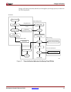
As a final test, you can verify how your design performs in the target application. In-circuit
verification tests the circuit under typical operating conditions. Because you can program
your Xilinx devices repeatedly, you can easily load different iterations of your design into
your device and test it in-circuit. To verify your design in-circuit, download your design
bitstream into a device with the Parallel Cable IV or MultiPRO cable.
Note:
For information about Xilinx cables and hardware, see the iMPACT online help.
Design Rule Checker (FPGAs Only)
Before generating the final bitstream, it is important to use the DRC option in BitGen to
evaluate the NCD file for problems that could prevent the design from functioning
properly. DRC is invoked automatically unless you use the –d option. See Chapter 8,
“Physical Design Rule Check” and Chapter 14, “BitGen” and for detailed information.
Xilinx Design Download Cables
Xilinx provides the Parallel Cable IV or MultiPRO cable to download the configuration
data containing the device design.
You can use the Xilinx download cables with the iMPACT Programming software for
FPGA and CPLD design download and readback, and configuration data verification. The
iMPACT Programming software cannot be used to perform real-time design functional
verification.
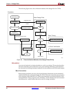
Probe
The Xilinx PROBE function in FPGA Editor provides real-time debug capability good for
analyzing a few signals at a time. Using PROBE a designer can quickly identify and route
any internal signals to available I/O pins without having to replace and route the design.
The real-time activity of the signal can then be monitored using normal lab test equipment
such as logic/state analyzers and oscilloscopes.
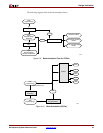
ChipScope ILA and ChipScope PRO
The ChipScope toolset was developed to assist engineers working at the PCB level.
ChipScope ILA actually embeds logic analyzer cores into your design. These logic cores
allow the user to view all the internal signals and nodes within an FPGA. ChipScope ILA
supports user selectable data channels from 1 to 256. The depth of the sample buffer ranges
from 256 to 16384 in Virtex-II devices. Triggers are changeable in real-0time without
affecting the user logic or requiring recompilation of the user design.